
The structures and morphologies of interest in condensed phases span a size range of about seven orders of magnitude, from atomic bond lengths $\mathrm{(10^{-10}\,m)}$ to thick layers deposited as coatings on engineering materials $\mathrm{(10^{-3}\,m)}$. In order to map a plane on the surface or within the specimen, we need to receive rays from the source which interact with different points in the specimen plane. If two points are too close together, the spherical waves emitted from these points interfere and we won't be able to resolve these points. If the wavelength is comparable to or larger than the structures investigated, the structures will not be imaged but rather cause scattering (i.e. diffraction or diffuse scattering). Since visible light has wavelengths of the order of $\mathrm{10^{-7}\,m}$, it can only be used to image structures near the top end of the morphology scale.
This limitation is known as the diffraction limit. It puts a lower limit on the size of structures that can be resolved using rays of a given wavelength, even if an optical system could be devised that is flawless and doesn't introduce any artefacts. The distance $d$ between two points on the sample surface that can be resolved as distinct is given by $$d=\frac{\lambda}{2n\sin\vartheta}\qquad,$$ where the refractive index, $n$, determines the resolving power of the (otherwise presumed ideal) instrument. In addition, the viewing angle $\vartheta$ also affects resolution via the numerical aperture, $n\sin\vartheta$, i.e. best results can be achieved when looking head on at the feature under study. This relationship can be derived by considering two overlapping Airy discs and the interference of the spherical waves emanating from two separate point sources. This is equivalent to the problem of using a telescope to resolve two stars in close proximity of each other.
In principle, we can extend the size range of resolvable structures by moving down the electromagnetic spectrum, towards the ultraviolet or even x-rays. The x-rays generated by a copper anode have a wavelength of about $\mathrm{1.5\times 10^{-10}\,m}$, comparable to the bond lengths in solids. Therefore, structures of tens of nanometres would be large enough to be reproduced by microscopy.
Alternatively, we can use sub-atomic particles, which have wave properties according to the wave-particle duality principle of quantum mechanics. This means that electron rays can be used for microscopy. For electrons, as for any quantum particle, we can calculate the de Broglie wavelength from the electron's momentum $$\lambda=\frac{h}{m_ev}=\frac{h}{\sqrt{2m_eeU}}\qquad,$$ using an accelerating voltage, $U$, to adjust the velocity and therefore the wavelength of the electrons: $$E_{kin}=\frac{1}{2}m_0v^2=eU=E_{el}\qquad.$$ A relativistic correction of the formula may be necessary at high voltages if the velocity becomes close to that of light.
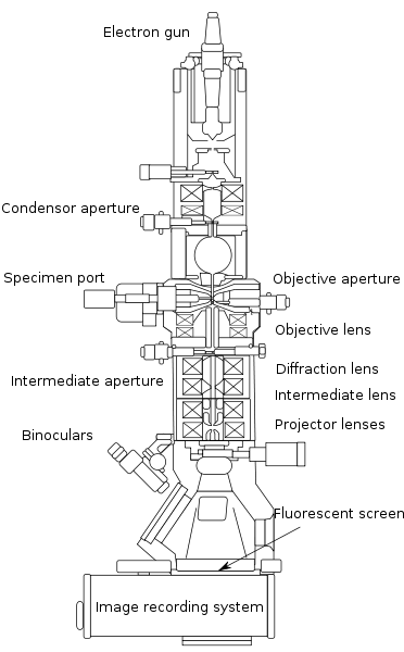
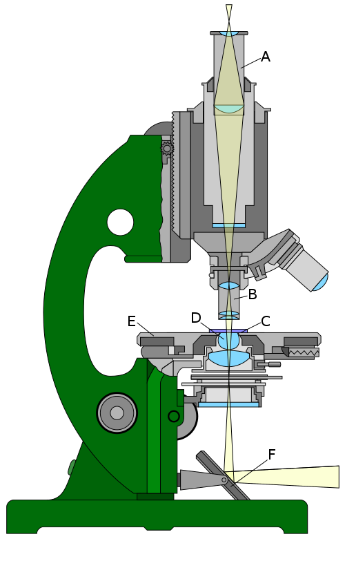
A transmission electron microscope (Fig. right) is essentially optically analogous to an optical microscope (Fig. left) using visible light. Of course various components have to be reworked in order to cope with the much shorter wavelength and the fact that electrons are charged particles as well as waves. The most obvious difference in the optical design is that the TEM has an upside-down optical path compared to the standard design of optical microscopes.
The wave source is an electron gun at the top rather than a lamp or mirror at the bottom. The electron gun typically is a lanthanum boride or tungsten filament which releases electrons by thermionic emission when heated.
Electrons are then accelerated downward by passing through a mesh capacitor, i.e. two wire meshes having different electrical potential, creating an electric field to accelerate the electrons in the downward direction. The potential difference is the accelerating voltage (of the order of hundreds of kV), which determines the de Broglie wavelength of the electrons as seen above.
Like the optical microscope, the TEM has a condensor or beam conditioning optic, which ensures that the area of interest on the sample is uniformly illuminated. Like all focusing elements in the TEM, this has to be realised by electrical and/or magnetic fields as conventional glass lenses would just absorb the electron beam rather than refract it. As in the optical microscope, the imaging optics comes in two pieces, the objective and ocular lenses, the latter magnifying an intermediate image created by the former.
An important difference is the method of perceiving the image generated. Since we lack a sensory organ to 'see' electrons, a fluorescent screen is used to generate a visible pattern by exciting dye molecules when hit by electrons. This is usually recorded with a CCD camera and viewed on a computer, although it is possible (and was common in early TEM instruments) to view the fluorescent screen through a pair of binoculars built into the base of the microscope.
In an optical microscope, the sample is placed in the beam by putting it on a glass microscope slide and positioning it manually. Since the whole beam path of the TEM must be in ultra-high vacuum to prevent the electrons from scattering with air molecules, the sample stage includes a transfer chamber in which the sample is placed and which is evacuated before the sample can be transferred into the main chamber. Sample positioning, which has to be much more precise than in an optical microscope because of the higher resolution, is by means of positioning stages based on stepper motors or piezo-devices.
As seen above, the wavelength of the electron can be adjusted via the accelerating voltage, $U$. At the same time, a voltage bias can also be used to focus the beam in an optical element. Effectively, a shaped capacitor acts in the same way on an electron beam as a glass lens does on a beam of visible light.
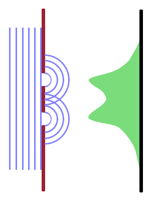
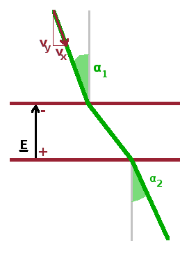
We can calculate what is effectively the refractive index of a capacitor by considering Snell's law and apply it to the situation of an electron beam in a capacitor. The analogy is clear when considering the refraction of an electron beam when it enters a mesh capacitor at an angle with the normal and when it leaves the capacitor again, in the same way a beam of visible light gets refracted when entering and again when leaving a sheet of glass under an angled exposure. The electric field affects only the forward component of the electron velocity, i.e. the lateral components are the same: $$v_{x,1}=v_{x,2}\qquad.$$ However, the forward component, $v_y$, of the velocity is changed by the electric field because the charged electron has to fly either in the direction of the electric field or against it.
In optics, Snell's law establishes that the sines of the incident and refracted angle have the same ratio as the (phase) velocities of the rays in the two media on either side of the refracting interface. Since the electron velocity is determined by the accelerating voltage via the kinetic energy of the electron, the velocity ratio can be replaced by the ratio of the square roots of the potentials of the two capacitor meshes: $$\frac{\sin\alpha_1}{\sin\alpha_2}=\frac{v_{x,1}/v_1}{v_{x,2}/v_2}=\frac{v_2}{v_1}=\sqrt{\frac{U_2}{U_1}}\qquad.$$ In visible optics, the refractive index is the ratio of the actual speed of light in the material and the speed of light in vacuum. Therefore, the refractive index of electron optics is the square root of the accelerating voltage: $$n=\sqrt{U}$$
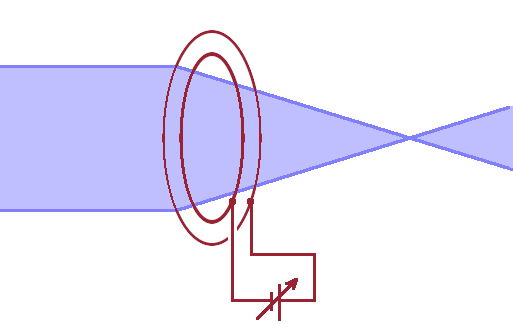
This can be exploited to build focusing optics for electron microscopes: An electrical immersion lens, i.e. a lens that focuses the beam onto a point in the sample plane, can be realised by a circular mesh electrode nested inside another, together forming the shape of a convex lens. The refractive index of the lens is then given by $$n=\sqrt{\frac{U_2}{U_1}}\qquad.$$ The focal length of such a simple convex lens is, according to geometrical optics, given by: $$\frac{1}{f}=\left(\sqrt{\frac{U_2}{U_i}}-1\right)\left(\frac{1}{r_1}+\frac{1}{r_2}\right)\qquad,$$ where $r_1$ and $r_2$ are the radii of curvature of the two meshes. By adjusting the potential difference between the two meshes, the focal length of the lens can be adjusted conveniently.
In practice, electrical electron lenses have a somewhat more complex cylindrical geometry because such a simple lens would also change the forward velocity of the electrons and thus their wavelength - changing the focus would therefore change the resolution simultaneously.
In addition to electrical electron lenses, there are also magnetic electron lenses based on the fact that charges are deflected if travelling through a magnetic field (Lenz's law - right hand rule). This is more often used to deflect a beam rather than to refract it, i.e. in cases where an electron beam is used to scan a region of the sample.
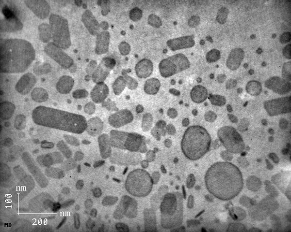
The simplest mode of operation of a TEM is bright field microscopy. This means that the image is simply a map of the shadow cast by structures in the sample due to their ability to absorb electrons. If there is no sample in the beam, the full primary beam hits the detector, resulting in a uniformly lit, bright image. This is also the most common mode of operation both of TEMs and of optical microscopes.
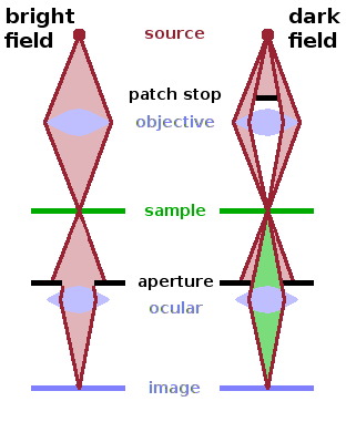
Alternatively, a small disc (the patch stop) can be inserted in the path of the direct beam. As a result, only rays away from the centre of the focusing element reach the sample. If they are transmitted through the sample without interaction, they will not reach the detector as they hit the sample at an angle off the normal and are discarded by the ocular aperture. If there is no sample in the beam, the result is a uniformly dark image. If a sample is present, rays that scatter within the sample may be diverted towards the detector and therefore contribute to the dark field image. Dark-field microscopy therefore highlights structures that are more likely to scatter electron rays, such as grain boundaries or other boundaries within an inhomogeneous sample. Dark-field microscopy is also sometimes used in optical microscopy to emphasise boundaries of regions with different refractive index. Of course the scattered rays are also contained in the bright-field image, but since they are a minority of the rays reaching the detector, the specific information they carry is lost in the image. On the other hand, this explains why dark-field images are much noisier - most incident electrons (or photons) are discarded by the patch stop.
A variation of dark-field imaging is microscopy using phase contrast. Here, the fact that the wavelength of two rays from the same source is different if they travel through media of different refractive index is exploited. When the two rays interfere after passing through parts of the specimen that have different refractive index, dark and light patterns emerge dependent on whether the rays interfere constructively or destructively. This can be used to visualise information that would not be visible in a bright-field image since regions of the sample may differ in refractive index while absorbing similar amounts of the incident beam.
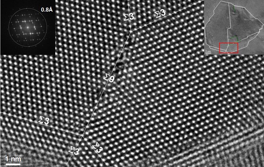
In high-resolution TEM, i.e. TEM with very high acceleration voltages and therefore low wavelengths, phase contrast can be exploited as diffraction contrast, where the incident wave interferes with the electron waves diffracted by the crystalline structure of the specimen. This technique is able to deliver atomic resolution, e.g. grain boundaries may be visualised using HRTEM. The Fig. shows a HRTEM image of a palladium crystal consisting of several grains with different orientiations along with the electron diffraction pattern recorded simultaneously (insert left).
Maximising resolution isn't always practical or even desirable since there is a trade-off between resolution and statistics. The big attraction of microscopy is that we can see what the specimen actually looks like at a certain level of structural detail. However, as we can take only so many images in the available time, we can never be certain that we won't miss an important feature either because it is rare enough that we don't sample it or because its size is such that it is too large or too small to be noticeable at the level of magnification used. This is a case of sample bias - we can only see features of the size we're looking for. It is therefore important to vary the magnification during any microscopy session and to sample a good range of locations within each specimen. Feature recognition algorithms can help remove some of this bias by drawing attention to features which may not be striking to the human eye.
Scattering techniques avoid these pitfalls of sample bias and limited statistical significance, alas at the price of requiring a model of the structure in order to interpret the scattering patterns. Therefore, microscopy and scattering are often used in conjunction: A structural model is developed based on microscopic analysis, and scattering patterns are analysed using that model to provide the necessary statistics.
The need to have samples that are thin enough to permit an electron beam to be partially transmitted makes sample preparation for TEM non-trivial. Typically, samples have to be 100nm thin at most. For specimens containing heavier elements such as transition metals, only a few tens of nm are feasible. While soft materials such as polymers or biological specimens can be sliced using an ultramicrotome (essentially a suitably stabilised knife blade) after embedding in a harder matrix, harder inorganic materials have to be ground and polished or etched to the required thickness. This can cause artefacts due to selective abrasion or dissolution. Focused ion beam (FIB) sources utilise a beam of heavy ions (e.g. gallium ions) to drill two parallel trenches into the specimen, leaving a thin free-standing section ready to be lifted off. This is particularly useful for hard materials, where a microtome would not be useable, or where a very precisely defined area within the specimen is to be analysed.
While the TEM is modelled on the optics of a classical optical microscope, there are other ways of utilising an electron beam to produce images of the structure of a material. These use a scanning mechanism similar to that used in a cathode-ray tube monitor (those clunky old TV or computer monitors built until the early 2000s...) and are more sensitive to the surface of a specimen.