
TEM and SEM are based on the interaction of an electron beam with a sample, either by analysing the selective absorptivity of regions of the sample (TEM) or by probing a variety of scattering mechanisms occurring as the beam is scanned across the sample.
Scanning probe microscopies, on the other hand, are based on the concept of an interaction between a fine tip of atomic dimensions with a sample surface. Different types of interaction can be utilised, but in all cases, an image of exclusively the surface topography of the sample is recorded point by point. The lack of depth information is usually considered an advantage rather than an impediment if topography is the object of study since it allows to concentrate on this aspect of the structure without having to filter out signal received from buried layers which may be difficult to distinguish.
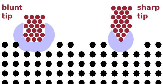
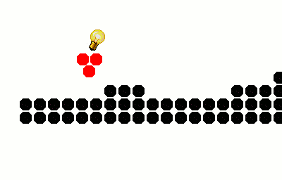
Scanning probe techniques rely on the use of an atomically sharp tip. These techniques measure interactions between atoms on either side of the gap between the tip and the specimen surface. If the tip is sharp, these interactions relate to specific atoms on either side of the gap which are closest to one another at any given moment, producing a crisp image with potentially atomic resolution. However, if the tip is blunt, there will be several atom pairs at similar distances, and as a result the image will be blurry at best. Tips therefore are consumables and have to be replaced when worn.
The two main scanning-probe techiques in general use are Scanning Tunnelling Microscopy (STM) and Atomic Force Microscopy (AFM).
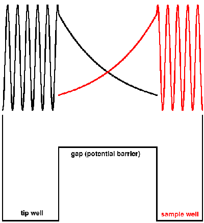
The scanning tunnelling microscope is based on the concept of quantum-mechanical tunnelling. The wave function of an electron in a square well can be obtained by solving the Schrödinger equation for a particle in a well. The boundary condition that requires the wave function to decay to zero at the edges of an infinite well forces the solution to be a sine wave. The probability density of the electron is proportional to the square of the wave function (shown in the top part of the figure).
In the case of a finite potential well (as in the case of the gap between tip and sample), the only boundary condition applying at the edge of the well is that the wave function is continuous. This means that the oscillatory function inside the well turns into a decaying exponential inside the barrier. The same situation occurs on the other side of the gap. The tunnelling probability depends on the overlap integral of the two decaying wave functions inside the barrier.
Of course a real tip or surface atom isn't simply a square well. This changes the precise shape of the wave function but not the underlying principle.
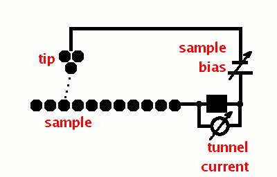
The basic idea is quite straightforward: Each of the surface atoms of the sample is a quantum well. A sharp tip with a single atom at its point is moved across the sample. A bias voltage is applied across the gap between tip and sample. If the tip is close enough to the surface, electrons from one side of the gap can tunnel through the finite potential barrier that is the gap and reach the atom (well) on the opposite side. As long as the bias is maintained a steady stream of single electrons is crossing the gap: the tunneling current.
The easiest way to scan a surface would be to move either the tip or the sample while measuring the tunnelling current. If there is an island on the surface, the tunnelling current would be enhanced because the gap would narrow correspondingly. Similarly, a groove in the surface leads to a widening of the gap and hence a decrease in the current.
The problem with this approach is that if the sample is terraced or the surface is slightly tilted, the tip will crash sideways into the obstacle and be destroyed. Since such effects are on the scale of the surface features to be observed, this would invariably occur in every single experiment at some stage.
To avoid this, the distance between the tip and the sample is adjusted continuously such as to keep the tunnelling current at a constant level. This requires a third piezo-driven axis in addition to the two scanning axes. It also requires electronics whose response time is fast enough to drive the $z$ piezo before the tip reaches the object that causes the increase in tunnel current.
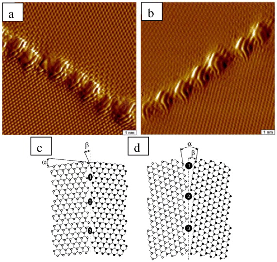
STM is capable in principle of delivering images with atomic resolution since it is not based on an interaction with waves and therefore doesn't have a diffraction limit. Of course there are some technical limitations to the available resolution such as image stabilisation (avoiding environmental vibrations), stray electric or magnetic fields, deformed imaging tips, or extraneous materials deposited on the surface. However, if these problems can be overcome, it is possible to image surface features such as grain boundaries (Fig.) depicting the positions of individual atoms. For STM to work with atomic resolution does require an undistorted periodic lattice structure because irregularities tend to cause loss of focus because they cause vibrations of the tip. This can be seen in the Fig., where the atoms involved in the grain boundary appear fuzzier than those in the undistorted grain interior.
One severe limitation of STM is that electrically conducting samples are required in order to produce a steady current across the gap between the tip and the sample.
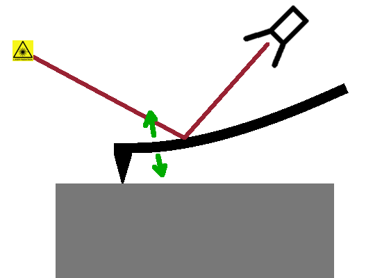
An alternative to STM that doesn't require samples to be electrically conducting is Atomic Force Microscopy (AFM). Here, an atomically sharp tip is attached to a thin, springy cantilever which bends as a result of the interatomic forces between the tip and atoms in the sample surface. This small dynamic response is magnified using a laser reflected at the back of the cantilever; the extent of deflection of the laser beam is a measure of the strength of the interaction of the tip with the sample.
AFMs can operate in three different modes depending on how close the tip comes to the surface. Given that the interaction between the tip and the surface is effectively the transient formation of a chemical bond, it is difficult to say when exactly the tip is 'in contact' with the sample. However, in the terminology used, contact mode means that a full chemical bond is formed between the tip atom and an atom in the surface of the sample, which essentially means that the tip gets as close as the repulsive component of the interatomic force will allow. This causes the largest possible deflection of the tip cantilever, but the strong interaction between the tip and the sample can easily lead to damage to both and thus to artefacts. In tapping mode, the cantilever oscillates with its own resonant frequency. As the tip approaches the surface in the course of this oscillation, the interaction with the surface increases and wanes periodically. The resonant frequency is removed from the signal, and the difference is representative of the strength of interaction. This mode is less taxing on the tip and the sample. Finally, for very delicate samples, it is possible to use non-contact mode and avoid the temporary formation of chemical bonds altogether. In this case, only weak long-range interactions such as the van-der-Waals force are monitored. Of course, the deflections are less prominent in this case, leading to a weaker and typically fuzzier image. AFM copes well with ambient conditions, and it is even possible to image surfaces covered with a thin liquid film.
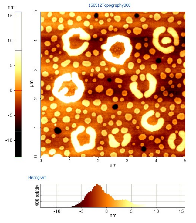
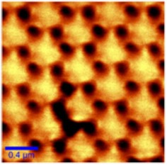
AFM images are false colour images (as are STM images), i.e. the colour shown represents the deflection of the tip within a range of values. AFM images reflect the topography of the surface of the sample, without any information about sub-surface features.
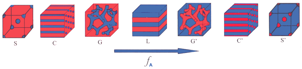
The AFM images (Figs.) show the surface of a diblock co-polymer film on a silicon substrate after exposure to different solvent vapours, causing different morphologies to prevail. The open rings ('henges') and white circles represent structures which protrude from the baseline height, while the black circles are small holes in the film. A histogram shows the distribution of pixels at a given height within the area sampled.
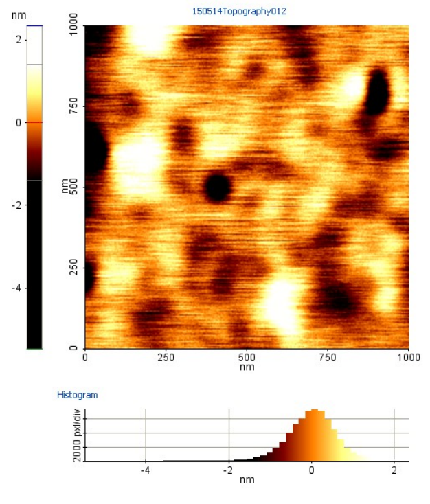
Images typically have to be processed to remove scanning artefacts such as fluctuations in the background height from which islands and depressions in the surface are measured as well as distortions caused by large objects which bend the cantilever to such an extent that it cannot flip back to its relaxed position immediately after the tip has passed the obstacle. Any features which appear to be exactly horizontal, i.e. follow the direction of scanning, are generally suspect and need to be investigated by rotating the sample.
Optical microscopy and TEM both rely on the fact that the objects to be imaged are larger than the wavelength of the probing wave. The resolution is limited by the diffraction limit. However, there is a way around the diffraction limit, enabling the use of visible light to probe surface structures much smaller than its wavelength. This is based on the detection of light in the near field, i.e very close to the sample surface.
When a ray of light hits a boundary between an optically denser and lighter medium, the ray is refracted away from the normal to the boundary. This is described by Snell's law, $$\sin\theta_2=\frac{n_1}{n_2}\sin\theta_1\qquad,$$ where $n$ is the refractive index and $\theta$ the angle of the ray with respect to the normal, while subscript 1 refers to the incident side and subscript 2 to the refracted side. Since $n_1\gt n_2$, there is an incident angle $\theta_c$ (known as the critical angle) where the right-hand side of the equation becomes greater than 1. This is the situation known as total internal reflection. In this case, Snell's law breaks down because the sine function on the left hand side can only take values from -1 to +1. This is resolved by considering the wave as a complex function, whereas Snell's law only considers the real component. Incident angles above the critical angle then cause $\cos\theta_2$ to become imaginary.
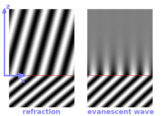
The electric field beyond the boundary is a function oscillating in both time and space: $$\vec{E}_2\propto\exp{\left({\rm i}(\vec{k}_2\vec{r}-\omega t)\right)}\qquad,$$ where $\vec{k}_2$ is the refracted wavevector, $\vec{r}$ contains the spatial co-ordinates, $\omega$ is the frequency and $t$ time. The scalar product in the spatial component can be split into the two components within ($x$) and normal ($z$) to the optical boundary: $$\vec{E}_2\propto\exp{\left({\rm i}(k_2\sin\theta_2x+k_2\cos\theta_2z-\omega t)\right)}\qquad.$$ Given that $\cos\theta_2$ is imaginary, it combines with the imaginary unit of the complex exponential function to produce a real exponential decay normal to the interface, while an oscillating solution prevails for the component aligned along the boundary and also for the temporal component. This pattern of wave propagation along the boundary with a vanishing electrical field into the lighter medium is known as an evanescent wave, and it allows us to bypass the diffraction limit by detecting light in the decaying electrical field just inside the lighter medium. As there is no oscillation in the direction normal to the boundary, waves will not interfere in that direction either.
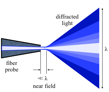
To do so, a very pointed optical fibre is scanned across the sample surface in the same way the tip of an AFM is. A z-scan mechanism is used to maintain a constant distance between the tip and the sample. The distance is kept significantly smaller than the wavelength of the light used in order to remain within the near field. The aperture of the fibre must also be smaller than the wavelength to avoid pinhole diffraction of the light emitted from the fibre.
Resolutions down to tens of nm are achievable with this technique, which is at least an order of magnitude below the wavelength of the light used. However, as is the case with all scanning probe techniques, the method is limited to scanning the surface topography of a sample. Images of buried features aren't possible.
The following table summarises some aspects of the microscopy techniques covered here.
| TEM | SEM | STM | AFM | SNOM | |
|---|---|---|---|---|---|
| probe | electron beam | electron beam | tip | tip | tip |
| image formation | direct | scanning | scanning | scanning | scanning |
| interaction | absorption | various | electron tunnelling | interatomic force | near field optical |
| resolution | Å-μm | nm-mm | Å-μm | Å-μm | 50-500nm |
| depth information | depth focus | sub-surface | none | none | none |
| chemical specificity | no | possible | no | limited | none |
| sample req. | very thin | conducting surface | conducting | any | any |
| artefacts | charging, obscuration | charging | tip damage | tip damage | tip damage |
This concludes the section on microscopy techniques supporting condensed matter physics. We will next expand on the topic of crystallography and diffraction covered in the Concepts lecture, starting from a brief review of the Bravais lattices used to describe crystal structures.