
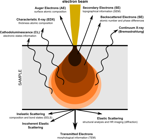
Apart from being absorbed, there is a variety of other ways for an electron beam to interact with a sample. Unlike TEM, which in its simplest form detects those electrons from an incident beam which have not interacted (i.e. are transmitted through the sample), other microscopy techniques concentrate on the products of that interaction. This includes photons as well as electrons emerging from the sample.
Depending on the interaction mechanism, electrons or photons may be emitted towards the source, i.e. the detectors will be placed above the sample and off-axis from the optical path from the source. These interactions therefore allow thicker samples to be used since there is no need for the beam to pass through the whole specimen. The interaction volume is the pear-shaped region on and below the surface of the sample in which detectable interactions take place. Depending on the interaction mechanism, this leads to different depth sensitivity for various techniques.
However, in all these techniques, the angle at which electrons or photons are emitted is variable, which means that the position at which an event is recorded on the detector isn't correlated with the position in the sample where the interaction took place. Therefore it is necessary to scan the electron beam across the sample surface to build up a raster image. This scanning of the sample surface is achieved by deflecting the electron beam using lateral magnetic fields in the same way a cathode-ray tube (CRT) monitor builds up an image on a fluorescent screen. This means the resolution of the image is no longer determined by the wavelength of the electrons and the depth of focus of the optics but rather by the step size of the scanning mechanism. All of these scanning techniques are variations of scanning electron microscopy (SEM). Depending on what detectors are used (and therefore what interaction is probed), it is possible to obtain images with chemical specificity, i.e. identify regions within a sample that contain certain chemical elements.
The main interaction types used in scanning electron microscopy and associated techniques are described below.
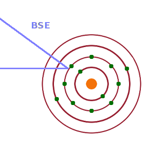
In backscattered electron (BSE) imaging, an electron from the source is scattered by an electron within an atom of the sample due to their mutual Coulomb repulsion. As a result, the incident electron is scattered at an arbitrary angle, and some of these electrons are scattered in a backward direction and can therefore be detected by a detector above the sample. While the incident electron will lose some energy in the scattering process, it will be ejected with much of its incident energy remaining. BSEs can therefore be scattered from relatively deep inside the sample, thereby including information about buried layers.
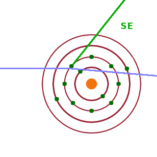
On the other hand, if an incident electron scatters with an electron present in the sample in such a way that the sample electron is ejected from its atom, this secondary electron is emitted from the sample with an energy reduced by its work function (ionisation energy). Due to their lower energy, such secondary electrons are more likely to be absorbed as they travel back to the surface of the sample. Therefore SE contrast is more concentrated on features on or only just below the surface than BSE contrast. In the detector, BSE and SE are distinguished by means of an energy discriminator: electrons below about 50eV are secondary electrons, while BSE have energies in the keV range depending on the accelerating voltage used.
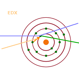
In addition to detecting electrons, photon (x-ray) detectors may be added to the SEM. This is known as energy-dispersive x-ray (EDX) detection. EDX applies if the hole in the electronic structure formed by the emission of a secondary electron is filled by an outer electron of the same atom dropping into the vacated level. The energy difference between the two electronic states involved is released as a photon, typically in the x-ray regime. Since the precise energy difference is a function of the structure of the electron shell of that particular atom, the energy of the emitted x-ray carries information about which chemical element is present. By combining the spectroscopic EDX information with the secondary-electron contrast image, it is possible to chemically analyse different regions of a sample.
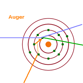
However, the x-ray emitted may be absorbed before it reaches the detector. If it gets absorbed immediately by another electron in the outermost shell of the same atom from which it was emitted, it may cause that electron to be ionised. Such electrons are called Auger electrons, and their precise energy is dependent not only on the element from which they are ejected but also the specific chemical environment in which the atom resides since the energy levels of outer electrons change due to the formation of chemical bonds with neighbouring atoms.
Since each of these processes successively build on the previous ones, the number of events detected are getting smaller as we switch from BSE, SE, EDX to Auger imaging. Therefore, the added chemical selectivity of the latter methods comes at the price of reduced statistics. It is also important to consider that information about the bulk of the sample can only be obtained by energetic electrons (BSE) or x-rays (EDX) as lower-energy electrons would not be able to make it back to the surface without being absorbed.
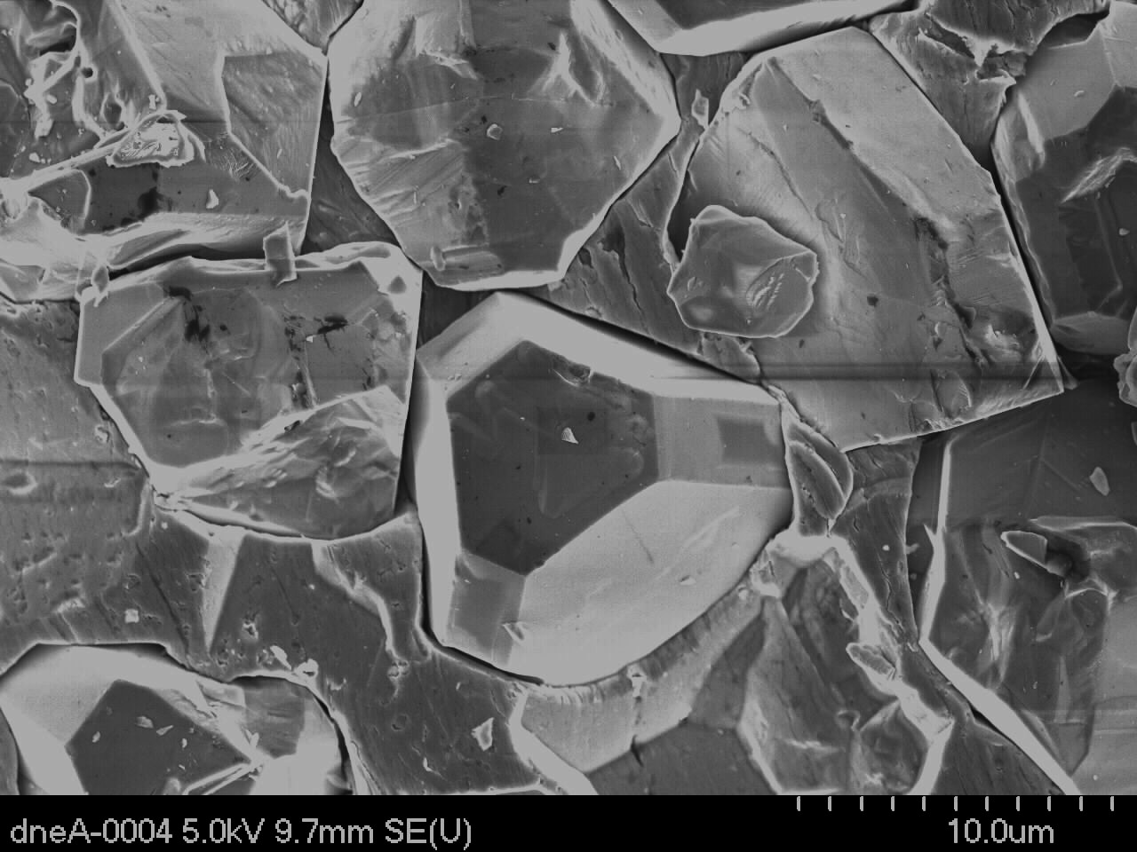
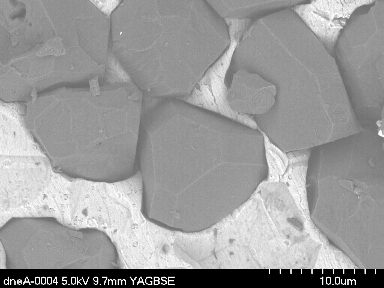
The two images compare the same region of a cubic boron nitride sample consisting of several individual crystals as seen under backscattered electron contrast (left) and secondary electron contrast (right). The SE image shows clearly the detail of the surface topography including the faceting of the crystals but it doesn't produce much contrast between the crystals and the less ordered matrix they're growing on. This is much easier to make out in the BSE image, which also records electrons scattered deeper inside the crystals.
Since the samples for SEM experiments can be quite thick (unlike TEM), charging effects can lead to artefacts. If the sample becomes charged up by absorbing electrons, it will deflect the electron beam, causing burnt out patches and lines along the scan direction in areas of the image that have been subjected to a focused electron beam if the samples aren't good electronic conductors. A (very mild) example of this can be seen on the right-hand side of the secondary electron image above. For insulating samples, a common remedy is to sputter a thin layer of conducting graphite on the surface of the sample. Since carbon is a very light element, it is fairly transparent even to secondary electrons, and a thin film shouldn't obscure the underlying topography too much.
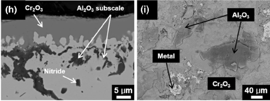
BSE really comes into its own when heterogeneous alloys are studied. This Fig. shows an oxide scale on an aluminium-chromium alloy with chemical contrast from BSE. The two elements have very different masses, making the heavier Cr a much more effective back-scatterer. As a result, the chromium-containing regions show brighter than those consisting of alumina. The unoxidised chromium grain in the right Fig. is even brighter since its Cr concentration is higher than that in the oxide. This information would be invisible in secondary electron contrast; at best the boundaries between the different phases might be seen, without being able to identify them as different in composition.
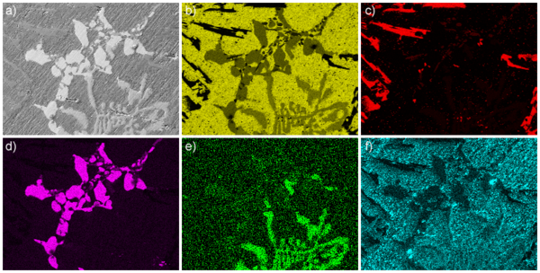
However, an analysis such as the one above is limited to assigning each grain to one of the phases known to be present. In an unknown substance, or if a semi-quantitative analysis of each grain is required, chemical contrast from EDX is needed. The Fig. shows the distribution of Al, Si, Cu, Fe, and O across the secondary-electron image top left. It becomes clear that Si (red) and Cu (purple) are totally segregated in this alloy, while Al (yellow) and iron (green) are present in all grains, although with variable concentrations. Sometimes, the false-colour images showing the concentrations of each element are superimposed on top of each other. The efficiency of x-ray emission scales with the square of the atomic number, which has to be taken into account when working out a quantitative analysis from the EDX intensity of the various elements.
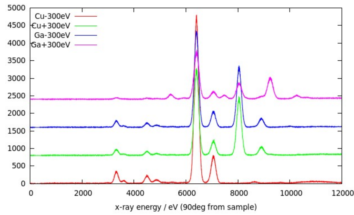
The composition map is only part of the information available with SEM-EDX. For each region, a full x-ray emission spectrum can be determined, showing the characteristic emission lines of each element present in the region with its relative strength. The Fig. shows the Kα and Kβ emission lines of potassium, iron, copper and gallium in a sample containing these elements (although this particular spectrum was recorded using incident x-rays rather than electrons to excite the emission). This demonstrates that an emission can only be excited if the source of the excitation is at least as energetic as the emission line itself.
While SEM with secondary electron contrast produces images heavily weighted towards the surface of the sample, surface topography can be studied exclusively by scanning probe microscopies.