Putting a lot of atoms together: solids


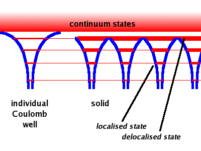
The Coulomb well potential of an individual atom has sharp energy levels - the states with different main quantum number n. At the top of the well, where the potential becomes very shallow, the distinct energy levels approach the continuum characteristic of a free electron.
When many such Coulomb wells are placed in a regular array (i.e. a crystalline lattice), two effects are observed. First, the potential barrier between adjacent atoms is lowered, allowing the electrons in states higher up the energy scale to delocalise across the crystal. These electrons have not enough energy to reach one of the continuum states outside the crystal, but their energy is sufficient to overcome the internal potential barrier between the atoms. This is exactly the same observation as in the case of forming a molecule from two Coulomb wells. Second, the sharp energy levels of the individual Coulomb well are replaced by energy bands. These bands are getting wider as the energy increases.
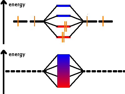
We have seen that, when linear-combining states, the number of states coming out of the process is always equal to the number of states put in. When forming a chemical bond between two atoms, two molecular states are generated (one bonding and one anti-bonding). By extension it follows that when four atomic states are combined, four molecular states ensue. These spread over the same range of energies; therefore the energy splitting between the states is smaller. Again, half the molecular states are bonding and the other half anti-bonding.
With many atoms in a crystal all contributing to the "molecular" states of the solid, there will be as many states as atoms contributing. All these states are squeezed into the same energy range as two or four states were previously. The density of states is so high that it is impossible to distinguish them: we have an energy band instead. The bonding states are at the bottom of the band, the anti-bonding ones at the top.
There is also another argument for the existence of energy bands. It is based on the uncertainty principle
between energy and time,  .
The tunnelling probability between adjacent Coulomb wells is much lower for the states at the bottom
of the wells (i.e. localised states) as the potential barrier is higher for electrons occupying
those states than for those higher up. Taking the time an electron stays localised in the same Coulomb
well as a measure for the time uncertainty, we can infer that the energy uncertainty for these localised
electrons is rather smaller than for the delocalised ones at the top of the Coulomb potential. This
qualitative argument confirms that the width of the energy bands increases with the energy itself.
.
The tunnelling probability between adjacent Coulomb wells is much lower for the states at the bottom
of the wells (i.e. localised states) as the potential barrier is higher for electrons occupying
those states than for those higher up. Taking the time an electron stays localised in the same Coulomb
well as a measure for the time uncertainty, we can infer that the energy uncertainty for these localised
electrons is rather smaller than for the delocalised ones at the top of the Coulomb potential. This
qualitative argument confirms that the width of the energy bands increases with the energy itself.
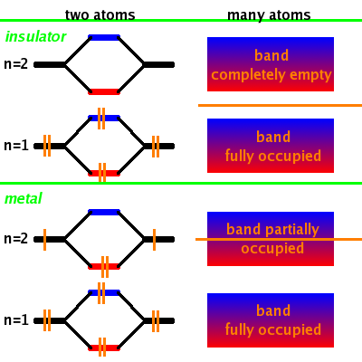
Consider a material where all states with a certain n are fully occupied with two electrons and all states at higher n are empty. When adding many atoms together, this results in a completely filled band at the lower n and an entirely empty one at the higher n. The cutoff between occupied and unoccupied states (the Fermi level, marked by an orange horizontal line in the Fig.) is between the two bands, i.e. within the bandgap. The upper band (the conduction band) is empty, the lower band (the valence band) is completely filled. Electrons can't move because there is no space for them to do so. This material is an insulator.
In another material, where the higher-n state is occupied by one electron, the corresponding band structure has a partially filled band, i.e. the Fermi level is within a band. In this case, the electrons can easily move as there are plenty of states available within the band at (almost) the same energy. This material is a metal.
A semiconductor is an insulator with a rather narrow bandgap, enabling some electrons to cross from the valence band into the conduction band after thermal activation. In an insulator, the temperature needed to excite significant numbers of electrons into the conduction band would melt the crystal; in a semiconductor, thermal activation is noticeable at room temperature or even below. Both electrons in the conduction band and the holes they leave behind in the valence band when making the transition are mobile and contribute to the conductivity. Sometimes both electrons and holes are coupled by their Coulomb attraction; they can then be treated as one complex particle, an exciton. More on this in 3rd year Solid State Physics.
 .
.